LED💡
INTRODUCTION
A p-n junction diode, which emits light on forward biasing, is known as light emitting diode. The emitted light may be in the visible range or invisible range and the intensity of light depends on the applied potential.
Theory
In a p-n junction charge carrier recombination takes place when the electrons cross from the n-layer to the P-layer. The electrons are in the conduction band on the p-side while holes are in the valence band on the p-side. The conduction band has a higher energy level compared to the valence band and so when the electrons recombine with a hole the difference in energy is given out in the form of heat or light. In case of silicon or germanium, the energy dissipation is in the form of heat, whereas in case of gallium-arsenide and gallium phosphide, it is in the form of light. But this light is in the invisible region & so these material cannot be used in the manufacture of LED. Hence gallium – arsenide phosphide which emits light in the visible region is used to manufacture an LED.
Construction
An n-type layer is grown on a substance and a p-type layer is grown over it by diffusion process. The P-layer is kept at the top because carrier recombination takes place in it. The terminals anode and cathode are taken out of the n-layer and P-layer respectively. The anode connections are made at the edge in order to provide more surface area for the emission of light. A metal film is applied to the bottom of substance to reflect light to the surface of the device and also to provide connection for the cathode terminal. Finally the structure are provided with an encapsulated (cover) to protect them from destruction
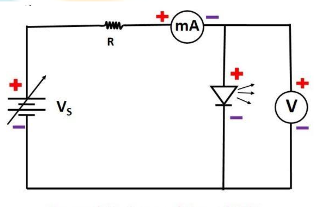
Circuit Diagram